process silicon mining
Silicon: mining and processing | Britannica
NARRATOR: Although the silicon in the rock is highly concentrated, it still needs to undergo a costly and energy-intensive purification process before it can be used industrially. In this plant in Kristiansand the clean quartz is processed into high-purity silicon. The rock is melted in a furnace at 4,000 degrees and the silicon purified even ...
دردشة على الإنترنت
Modeling the Process of Mining Silicon Through a Single ...
2014-6-19 · Silicon is one of the most used materials in these two industries. It is an inexpensive and abundant semiconductor. However, the process of producing pure silicon adds to the cost and most people do not understand how it is done. One of the first steps of producing silicon is a process called carbonthermic reduction. Silicon dioxide (SiO. 2
دردشة على الإنترنت
Modeling the Process of Mining Silicon Through a Single ...
2014-6-19 · Silicon is one of the most used materials in these two industries. It is an inexpensive and abundant semiconductor. However, the process of producing pure silicon adds cost, and it is generally unknown to the public. One of the first steps in producing silicon is a process called carbon-thermic reduction.
دردشة على الإنترنت
Silica Mining | Processing Equipment | Flow
2 天前 · Silica Sand Mining introduces. Foundry silica sand is the quartz as the main mineral composition, particle size of 0.020 mm to 3.350 mm refractory particles, according to the mining and processing methods of different can be
دردشة على الإنترنت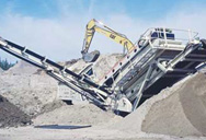
Mining And Refining: Pure Silicon And The Incredible ...
2021-11-15 · Polycrystalline silicon made by the Siemens process can have a purity of 99.99999% (“seven nines”, or 7N) or more. 7N to 10N polysilicon is mostly used for photovoltaic cells, although some ...
دردشة على الإنترنت
Impact of silica mining on environment
working on mining sites to understand the availability of basic amenities like water, health and sanitation to them, and nature, process and volume of silica mining in the area. He visited more than 50 mining sites to document the impact of large scale
دردشة على الإنترنت
(PDF) Silicomanganese Production - Process
2022-2-1 · The silicon content increases with the temperature and the silica content, and decreases with increasing R-ratio. The silicon content remains approximately the same when some MgO replaces CaO in ...
دردشة على الإنترنت
Silicon Hills Mining
Get into crypto mining at its most profitable time with a prebuilt, preconfigured mining rig! ... Ease of Use. We walk you through the entire process of setting up your mining web dashboard so you're ready to start mining as soon as your rig arrives. Management. ... Silicon Hills Mining Powered by Shopify. Payment methods Payment methods ...
دردشة على الإنترنت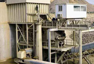
“Making of a Chip”
2018-1-9 · photolithography process just described. Then a chemical is applied to etch away unwanted silicon, leaving behind a fin with a layer of hard mask on top. Removing Photoresist – scale: transistor level (~50-200nm) The hard mask is chemically removed, leaving a tall, thin silicon fin which will contain the channel of a transistor.
دردشة على الإنترنتModeling the Process of Mining Silicon Through a Single ...
2014-6-19 · Silicon is one of the most used materials in these two industries. It is an inexpensive and abundant semiconductor. However, the process of producing pure silicon adds cost, and it is generally unknown to the public. One of the first steps in producing silicon is a process called carbon-thermic reduction.
دردشة على الإنترنت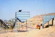
NEO Battery Materials’ silicon nano-coating process being ...
2021-8-13 · NEO Battery Materials’ silicon nano-coating process being tested for applicability in EVs. ... NEO is exploring and producing silicon at a number of
دردشة على الإنترنت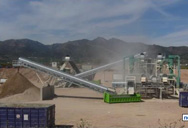
Silicon Wafer Manufacturing Process - Silicon
The stock removal process removes a very thin layer of silicon and is necessary to produce a wafer surface that is damage-free. On the other hand, the final polish does not remove any material. During the stock removal process, a
دردشة على الإنترنت
Silicon Ore - DSP Wiki
2021-7-24 · Player Tips & Tricks. While it is possible to process Silicon Ore from Stone on your home planet, this is a highly inefficient and timely method. Most starting star systems have at least one planet with Silicon Veins. Mining these allows for much faster production.
دردشة على الإنترنتProduction of raw silicon - Waferfabrication ...
The silicon reflects on the silicon rods which grow to bars with a diameter of more than 300 mm. This polysilicon could already be transformed into a single crystal using the Czochralski process, however, the degree of purity for
دردشة على الإنترنت
silicon from sand easy way - BINQ Mining
Silicon Information – Process Specialties Incorporated. The making of a Silicon wafer: With all this talk of sand and glass it may begin to The easy way to visualize Bow is if you think of the wafer as a bowl »More detailed
دردشة على الإنترنت
From Sand to Silicon - Intel
2018-1-9 · Silicon in the form of Silicon dioxide (SiO 2) and is the base ingredient for semiconductor manufacturing. Melted Silicon – scale: wafer level (~300mm / 12 inch) Silicon is purified in multiple steps to finally reach semiconductor manufacturing quality which is called Electronic Grade Silicon. Electronic Grade Silicon may only
دردشة على الإنترنت
Silicon Chips: What are Computer Chips Made Of?
2022-2-3 · A photolithographic "printing" process is used to form a chip’s multilayered transistors and interconnects (electrical circuits) on a wafer. Hundreds of identical processors are created in batches on a single silicon wafer. Once all the layers are completed, a computer performs a process called wafer sort test.
دردشة على الإنترنت“Making of a Chip”
2018-1-9 · photolithography process just described. Then a chemical is applied to etch away unwanted silicon, leaving behind a fin with a layer of hard mask on top. Removing Photoresist – scale: transistor level (~50-200nm) The hard mask is chemically removed, leaving a tall, thin silicon fin which will contain the channel of a transistor.
دردشة على الإنترنت
Silicon: leading producing countries ranking
Mining, Metals & Minerals. Average silicon prices in the U.S. by type 2016-2020 + Hardware. Semiconductor market size worldwide 2020-2030, by application + Mining, Metals & Minerals.
دردشة على الإنترنتModeling the Process of Mining Silicon Through a Single ...
2014-6-19 · Silicon is one of the most used materials in these two industries. It is an inexpensive and abundant semiconductor. However, the process of producing pure silicon adds cost, and it is generally unknown to the public. One of the first steps in producing silicon is a process called carbon-thermic reduction.
دردشة على الإنترنت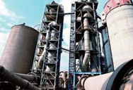
process for silica quartz to metallurgicalgrade silicon
Silicon, Silica, Silicates and Silicone » what is the process of mining quartz from the earth? ... extraction of silicon from silica ... What Is the Process of Mining Silicon ... Get More; processing plant high grade silica « gravel crusher sale.
دردشة على الإنترنت
Silicon Wafer Manufacturing Process - Silicon Valley ...
The stock removal process removes a very thin layer of silicon and is necessary to produce a wafer surface that is damage-free. On the other hand, the final polish does not remove any material. During the stock removal process, a haze forms
دردشة على الإنترنت
small process of extraction of silicon from quartz - BINQ ...
A new electrochemical process for silicon extraction could make »More detailed. Quartz Mining – Encyclopedia of Arkansas. Characteristics of Quartz Quartz is composed of silicon and This process can be as well as “rockhounds” who pick up small amounts of quartz from ...
دردشة على الإنترنت
Silicon seduced from silica | Nature
2003-5-19 · The process, developed by Toshiyuki Nohira and colleagues at Kyoto University in Japan, uses electricity to strip oxygen from silica, the
دردشة على الإنترنت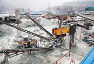
How Is Silicone Produced? - SIMTEC
2022-2-10 · Isolating silicon from silica is the first step in the production of silicone. This is done by heating a large volume of quartz sand to temperatures as high as 1800˚C. The result is pure, isolated silicon, which is allowed to cool and then ground into a fine powder. To make silicone, this fine silicon powder is combined with methyl chloride ...
دردشة على الإنترنتFrom Sand to Silicon - Intel
2018-1-9 · Silicon in the form of Silicon dioxide (SiO 2) and is the base ingredient for semiconductor manufacturing. Melted Silicon – scale: wafer level (~300mm / 12 inch) Silicon is purified in multiple steps to finally reach semiconductor manufacturing quality which is called Electronic Grade Silicon. Electronic Grade Silicon may only
دردشة على الإنترنتSilicon Chips: What are Computer Chips Made Of?
2022-2-3 · A photolithographic "printing" process is used to form a chip’s multilayered transistors and interconnects (electrical circuits) on a wafer. Hundreds of identical processors are created in batches on a single silicon wafer. Once all the layers are completed, a computer performs a process called wafer sort test.
دردشة على الإنترنتSilicon: leading producing countries ranking 2020 | Statista
Mining, Metals & Minerals. Average silicon prices in the U.S. by type 2016-2020 + Hardware. Semiconductor market size worldwide 2020-2030, by application + Mining, Metals & Minerals.
دردشة على الإنترنت“Making of a Chip”
2018-1-9 · photolithography process just described. Then a chemical is applied to etch away unwanted silicon, leaving behind a fin with a layer of hard mask on top. Removing Photoresist – scale: transistor level (~50-200nm) The hard mask is chemically removed, leaving a tall, thin silicon fin which will contain the channel of a transistor.
دردشة على الإنترنت
- inclined vibrating screening
- vibrating screen for crusher
- iron ore wet grinding and filtration
- digunakan kapur pemasok crusher dampak nigeria
- mining ore iron ore grinding mills
- allis chalmers cone crusher manual
- small cone crushers south africa
- daftar harga terkait
- feldspar extraction process
- stone crusher with best quality price
- conveyor belt tips
- stone crusher and mining in india
- hand coal mining crushers in zimbabwe
- grinding mill gold ore plant
- mongolia heavy hammer crusher